improved Yield prediction
by
by
new E-metrology tools for semiconductors
inline capability:
- non destructive
- topographic
- fast (up to one wafer / second)
- enables single wafer controll
|
prediction of device parameters before wafer processing |
|
|
|
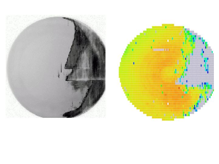
MDP liefetime scan, 6" silicon wafer as optained from manufacturer (left)- allows for the prediction of key parameters of final devices (right) |
scope
The worldwide rapidly growing progress in the development and manufacture of more and more sophisticated microelectronic semiconductor devices along with the necessity of high production yields call for powerful measurement tools in order to check quality parameters of the semiconductor materials used, e.g. wafers.Although extreme efforts are made to push the production technology of wafers and devices along with the most advanced test facilities to the limits, it is simply a fact that always too many devices fail or do not meet specifications.
Performance of semiconductor devices depends fundamentally on key electrical parameters of the material such as mobility, lifetime, and diffusion length of minority charge carriers.
However, only surprisingly little attention is paid so far to those dependencies along production lines. This is apparently also a consequence of so far insufficient metrology tools.
However, several breakthroughs were recently achieved. By the application of widely advanced microwave techniques it is now possible to measure the above mentioned electrical parameters ‘without touching the wafer’ with a so far unsurpassed combination of spatial resolution, sensitivity, and measurement speed.